
Semiconductor History | Maydan Technology Center — The Fab That Proves the Machines
· 2002-3
Personal memoryBy kevin · · updated · Report an issue
















































Find memories left by people near you.
Distribute Bounty
This will distribute the bounty equally among all qualifying memories. This action cannot be undone.
Cancel Bounty
Are you sure you want to cancel this bounty? The remaining amount will be refunded to your account.
Success!
Operation completed successfully.
Error
Something went wrong.
Semiconductor History | Maydan Technology Center — The Fab That Proves the Machines
kevin
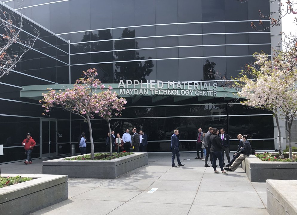
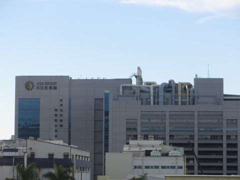
Applied Materials runs a wafer fab in Sunnyvale that exists to test the machines rather than to make product.
The Maydan Technology Center opened in March 2002 with 39,000 square feet of ISO Class 3 cleanroom inside a 166,000-square-foot building, and space for more than three hundred pieces of process and support equipment, which made it the largest process facility any equipment supplier ran.
Its product is confidence.
An etcher or a deposition chamber is not something a chipmaker can evaluate from a brochure. It has to run on real 300-millimetre wafers, through real process steps, before anyone commits a fab's ramp schedule to it.
So Applied built a place where a customer's engineers sit beside Applied's engineers and put the tool through its paces on silicon that will be thrown away.
The building carries the name of Dan Maydan, who was Applied's president when it opened and who is the executive quoted in the announcement.
By the company's current description the centre holds over 120 process tools and around 80 metrology and inspection instruments, absorbs roughly US$100 million of reinvestment a year, and runs around the clock with more than five hundred Applied engineers working alongside customers on nodes two generations ahead of production.
One correction is worth making here, because it is repeated almost everywhere, including on the Wikimedia file this photograph came from.
The Maydan Technology Center is in Sunnyvale, not Santa Clara. Applied's corporate address is Santa Clara, the two cities touch, and the trade press has copied the wrong one for twenty years; the building stands at 978 East Arques Avenue.
Something much larger is going up on the same Sunnyvale site.
Applied announced the EPIC Center in May 2023, a roughly US$5 billion research facility it calls the largest investment ever made in American semiconductor equipment research, with Samsung and SK hynix named as partners in early 2026 and an opening the company still places in 2026. Bloomberg reported in June 2026 that Applied had been told it would not receive CHIPS Act funding for it.
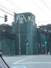
For now, what a visitor sees from Arques Avenue is a black glass building with a green awning and the name over the door.
Photo: Olaf2, CC BY-SA 4.0, via Wikimedia Commons.


changes?
delete this memory?
We detected that you have a Blox in your crypto wallet! We will import the Blox into your account.
Click on done below to complete the import.
Welcome Back!
Sign in to preserve cherished moments
Don't have an account?
Welcome!!
Sign up and start preserving cherished moments
?
?




Choose your payment method
Buy with Metablox Credit
Do you want to mint Blox with Metablox Credit?
Which Crypto would you like to use?
Purchase Confirmed!
Your Blox is being minted on-chain and will appear in your profile shortly.
Log in or sign up to claim your Blox.
How many credits do you want to buy?
$100 USD = 1 Metablox Credit = 1 Blox.
Use Metablox Credit to mint any Blox you want on the map.
 expand_more