


Semiconductor History | Intel Ocotillo, 25 October 2007 — Hafnium Replaces the Leaking Gate
· 2007-10
Personal memoryBy kevin · · Report an issue









































































Find memories left by people near you.
Distribute Bounty
This will distribute the bounty equally among all qualifying memories. This action cannot be undone.
Cancel Bounty
Are you sure you want to cancel this bounty? The remaining amount will be refunded to your account.
Success!
Operation completed successfully.
Error
Something went wrong.
Semiconductor History | Intel Ocotillo, 25 October 2007 — Hafnium Replaces the Leaking Gate
kevin
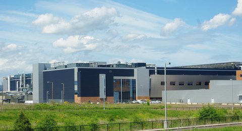
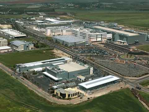
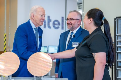
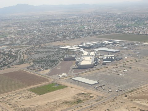
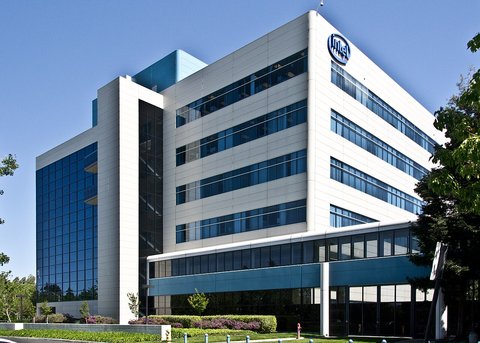
On 25 October 2007, Intel opened Fab 32 at its Ocotillo campus in Chandler, Arizona, for high-volume production on the 45-nanometer process. The $3 billion factory covered about one million square feet, including 184,000 square feet of cleanroom space, and became Intel’s sixth 300 mm wafer fab.
The landmark was not simply smaller geometry. Intel replaced the transistor gate’s increasingly leaky silicon-dioxide insulator with a hafnium-based high-k material and replaced the polysilicon gate electrode with metal, a paired materials change that restored electrical control as conventional scaling approached a barrier.
High-k dielectric reduced gate leakage, while the metal gate avoided performance loss associated with polysilicon depletion. Intel’s Oregon development fab had begun early production, but Fab 32 turned the recipe into volume manufacturing and helped establish Intel’s renewed process lead.
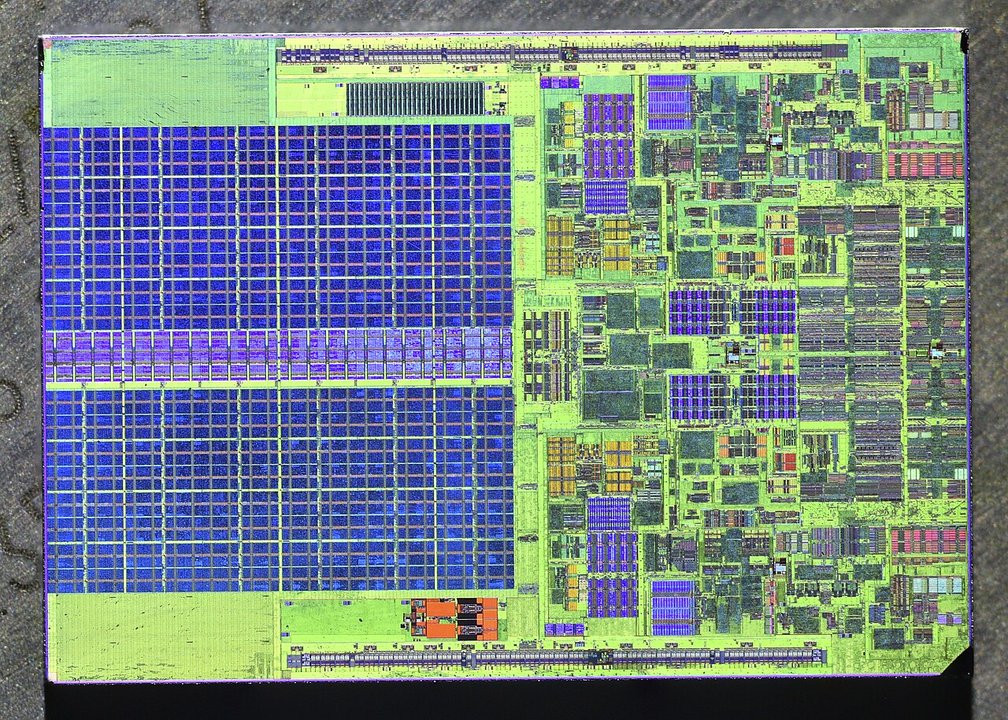
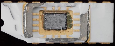
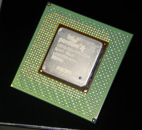
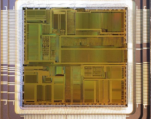
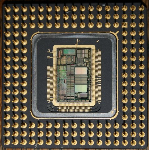
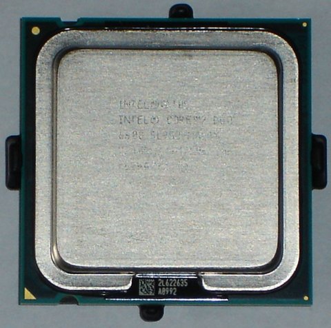
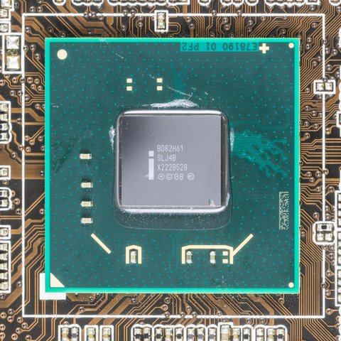
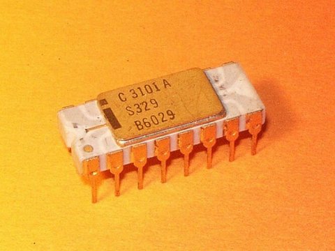
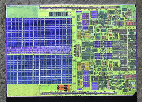
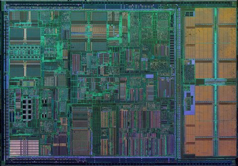
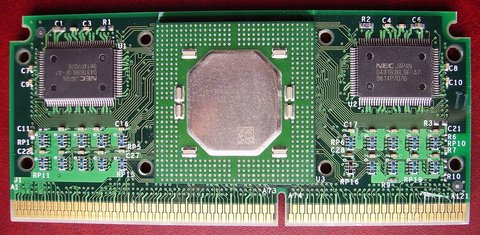
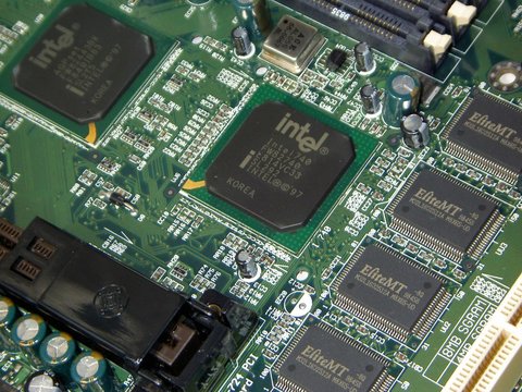
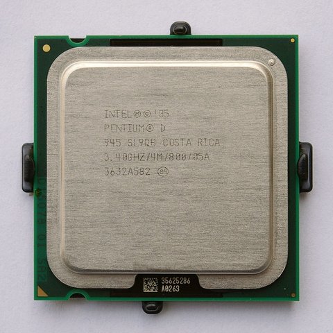
The first announced 45 nm family included sixteen Xeon, Core 2 Extreme, and related processors; some designs reached 820 million transistors. The photographed die is a later Wolfdale E8400 desktop member of that 45 nm generation, not a Fab 32 opening-day wafer, but it shows the physical product of the process transition.
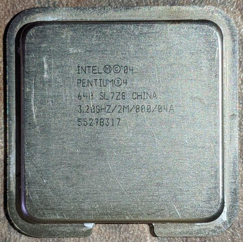
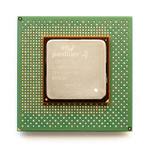
The good was a new lease on transistor scaling. Lower leakage and smaller transistors enabled denser chips with better power characteristics, letting Intel improve performance without relying only on the clock-frequency race that had run into thermal limits during the Pentium 4 era.
The bad was rising complexity and capital concentration. New gate materials, metal integration, contamination control, and a $3 billion production facility demanded extraordinary coordination; each successful shrink made the next manufacturing mistake more costly and made leading-edge competition harder for firms without comparable scale.
Intel did not invent the entire field of high-k research, which involved universities, suppliers, and competing chipmakers. Its achievement here was industrial: selecting a workable materials stack and putting it into high-volume logic processors, proving that one of silicon manufacturing’s most feared scaling obstacles could be crossed—at a price few companies could afford.
Photo: Martijn Boer, public domain, via Wikimedia Commons














changes?
delete this memory?
We detected that you have a Blox in your crypto wallet! We will import the Blox into your account.
Click on done below to complete the import.
Welcome Back!
Sign in to preserve cherished moments
Don't have an account?
Welcome!!
Sign up and start preserving cherished moments
?
?






Choose your payment method
Buy with Metablox Credit
Do you want to mint Blox with Metablox Credit?
Which Crypto would you like to use?
Purchase Confirmed!
Your Blox is being minted on-chain and will appear in your profile shortly.
Log in or sign up to claim your Blox.
How many credits do you want to buy?
$100 USD = 1 Metablox Credit = 1 Blox.
Use Metablox Credit to mint any Blox you want on the map.
 expand_more