


Semiconductor History | Intel Rio Rancho, 23 October 2002 — Twelve-Inch Wafers Change the Economics of a Fab
· 2002-10
Personal memoryBy kevin · · Report an issue










































































Find memories left by people near you.
Distribute Bounty
This will distribute the bounty equally among all qualifying memories. This action cannot be undone.
Cancel Bounty
Are you sure you want to cancel this bounty? The remaining amount will be refunded to your account.
Success!
Operation completed successfully.
Error
Something went wrong.
Semiconductor History | Intel Rio Rancho, 23 October 2002 — Twelve-Inch Wafers Change the Economics of a Fab
kevin
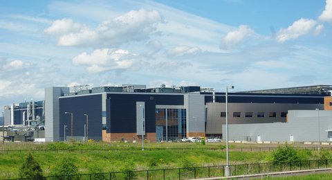
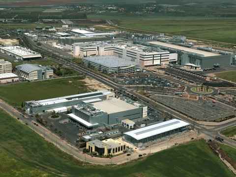
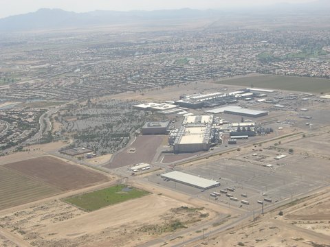
On 23 October 2002, Intel opened a $2 billion expansion called Fab 11X at its Rio Rancho, New Mexico, campus. The million-square-foot facility included roughly 200,000 square feet of cleanroom space and became Intel’s second factory to manufacture chips on 300-millimeter wafers.
The move from 200 mm to 300 mm wafers changed factory economics. Intel said the larger discs offered 225 percent of the surface area and could yield about 240 percent as many printed die, while using less water, energy, and other resources for each chip produced.
Fab 11X began with Intel’s 0.13-micron process and was prepared to move to 90 nanometers. It also embodied the “Copy Exactly” manufacturing discipline: process recipes and factory methods developed in Oregon could be reproduced in a high-volume site, shortening the path from laboratory achievement to millions of saleable processors.
The good was formidable productivity. More chips per wafer and lower cost per chip helped keep increasingly complex processors economically manufacturable, while a common 300 mm platform supported automated handling and a generation of process improvements.
The bad was the financial threshold. A $2 billion fab made semiconductor manufacturing more efficient only when it stayed highly utilized; the same scale raised the stakes of forecasting errors, narrowed the field of companies able to compete at the leading edge, and tied local employment to global production decisions.
A 2014 U.S. Labor Department decision later linked layoffs at the Rio Rancho site to shifts in CPU and chipset production outside the United States. Intel has since redirected the New Mexico campus toward advanced packaging and interconnect work, showing how an expensive manufacturing site must be repeatedly reinvented when its original process generation ages.
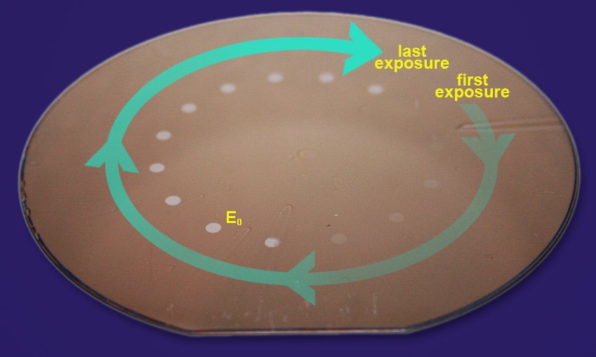
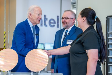
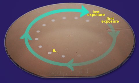
The pin marks the named public approach on Intel Drive near the official 1600 Rio Rancho Boulevard address, not a cleanroom entrance. The pictured 300 mm wafer comes from a later NIST photoresist experiment, not Fab 11X; its annotations document exposures while its scale makes the twelve-inch manufacturing transition tangible.
Image: National Institute of Standards and Technology, public domain, via Wikimedia Commons

















changes?
delete this memory?
We detected that you have a Blox in your crypto wallet! We will import the Blox into your account.
Click on done below to complete the import.
Welcome Back!
Sign in to preserve cherished moments
Don't have an account?
Welcome!!
Sign up and start preserving cherished moments
?
?




Choose your payment method
Buy with Metablox Credit
Do you want to mint Blox with Metablox Credit?
Which Crypto would you like to use?
Purchase Confirmed!
Your Blox is being minted on-chain and will appear in your profile shortly.
Log in or sign up to claim your Blox.
How many credits do you want to buy?
$100 USD = 1 Metablox Credit = 1 Blox.
Use Metablox Credit to mint any Blox you want on the map.
 expand_more