


Semiconductor History | 365 East Middlefield Road, 15 June 1970 - The Memory Chip You Could Erase and Try Again
· 1970-6
Personal memoryBy kevin · · updated · Report an issue






























































Find memories left by people near you.
Distribute Bounty
This will distribute the bounty equally among all qualifying memories. This action cannot be undone.
Cancel Bounty
Are you sure you want to cancel this bounty? The remaining amount will be refunded to your account.
Success!
Operation completed successfully.
Error
Something went wrong.
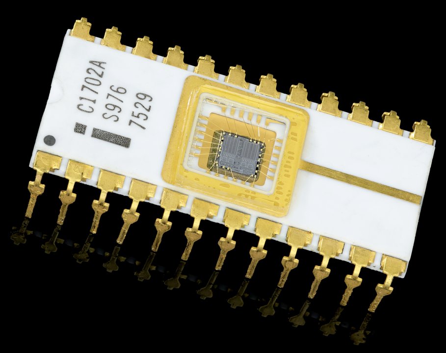
Semiconductor History | 365 East Middlefield Road, 15 June 1970 - The Memory Chip You Could Erase and Try Again
kevin
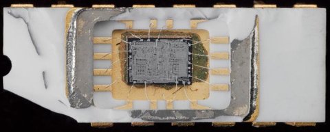
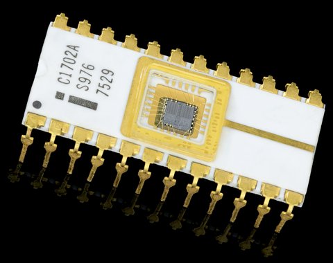
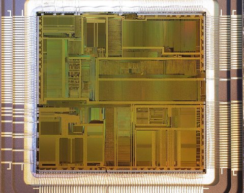
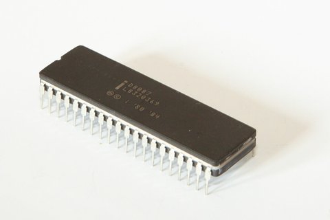
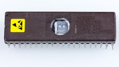
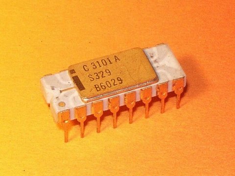
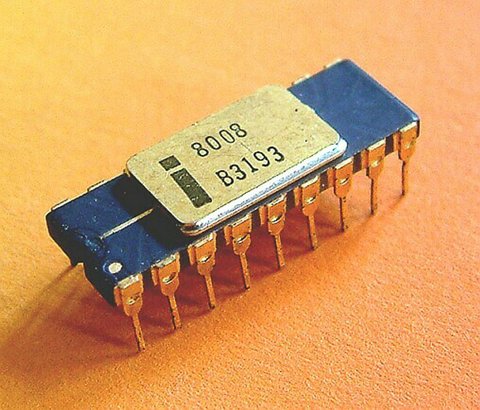
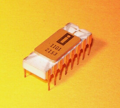
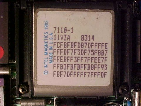
The gold wires inside this ceramic package lead to a small silicon die, visible because the protective quartz window has been removed.
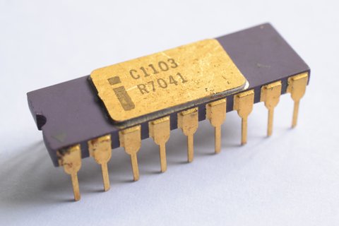
It is a later C1702A, a close relative of the device Dov Frohman developed at Intel when changing a program stored on a chip usually meant replacing the chip. The window normally let ultraviolet light reach the die and erase its contents so it could be programmed again.
On 15 June 1970, Frohman-Bentchkowsky filed the patent from Intel's first office at 365 East Middlefield Road in Mountain View. The patent assigned the invention to Intel and described a floating-gate memory cell that could retain information without power, accept new information electrically, and be cleared by radiation.
Intel introduced the 1702 in February 1971, when Frohman demonstrated the technology at the International Solid-State Circuits Conference. Computer History Museum records describe the commercial part as a 2,048-bit memory organized as 256 eight-bit words.
Its practical contribution was iteration.
A designer developing a controller or early microcomputer could change firmware without ordering a new mask-programmed ROM for every revision. That shortened the loop between finding an error, altering code, and testing the machine again.
The credit has an important boundary.
Dawon Kahng and Simon Sze at Bell Labs had described the floating-gate storage concept in 1967. Frohman's achievement at Intel was the working architecture and commercial product that made electrically programmable, ultraviolet-erasable nonvolatile memory useful to customers, not the first conception of a floating gate.
EPROM also carried costs that later technologies exposed. Erasure required removing the chip and shining ultraviolet light through its window for minutes, while the special ceramic package added expense; EEPROM and flash eventually made erasure electrical and more convenient.
Yet the transparent window became one of semiconductor history's most recognizable details. It made a normally invisible property physical: information could remain when the power disappeared, then be deliberately cleared so a machine could learn a different program.
Photo: Mister rf, CC BY-SA 4.0, via Wikimedia Commons. The pictured C1702A is a later package, not the specimen used for the 1970 patent filing.










changes?
delete this memory?
We detected that you have a Blox in your crypto wallet! We will import the Blox into your account.
Click on done below to complete the import.
Welcome Back!
Sign in to preserve cherished moments
Don't have an account?
Welcome!!
Sign up and start preserving cherished moments
?
?





Choose your payment method
Buy with Metablox Credit
Do you want to mint Blox with Metablox Credit?
Which Crypto would you like to use?
Purchase Confirmed!
Your Blox is being minted on-chain and will appear in your profile shortly.
Log in or sign up to claim your Blox.
How many credits do you want to buy?
$100 USD = 1 Metablox Credit = 1 Blox.
Use Metablox Credit to mint any Blox you want on the map.
 expand_more