


Semiconductor History | 365 East Middlefield Road, 1969 — Intel's 1101 Turns a Commercial Disaster Into a Process
· 1969
Personal memoryBy kevin · · Report an issue







































































Find memories left by people near you.
Distribute Bounty
This will distribute the bounty equally among all qualifying memories. This action cannot be undone.
Cancel Bounty
Are you sure you want to cancel this bounty? The remaining amount will be refunded to your account.
Success!
Operation completed successfully.
Error
Something went wrong.
Semiconductor History | 365 East Middlefield Road, 1969 — Intel's 1101 Turns a Commercial Disaster Into a Process
kevin
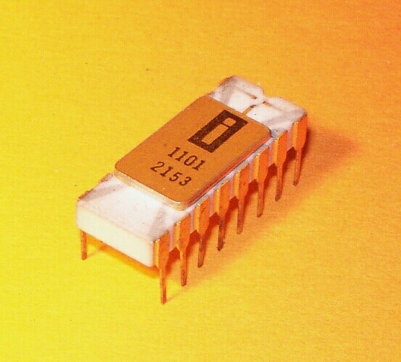
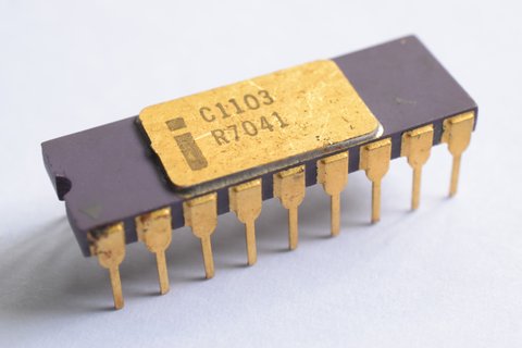
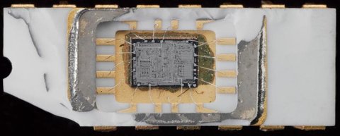
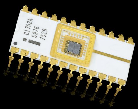
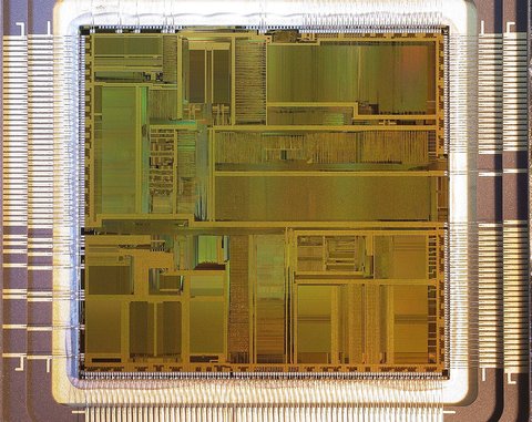
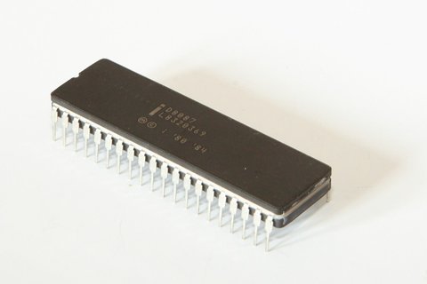
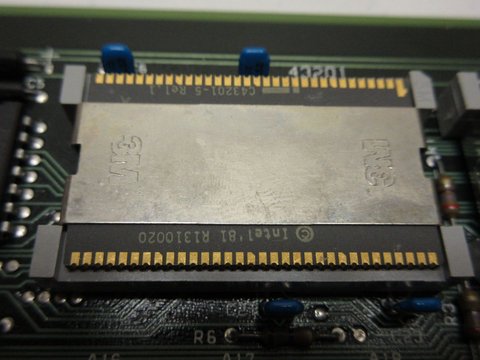
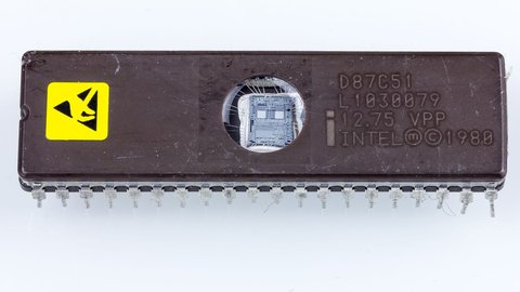
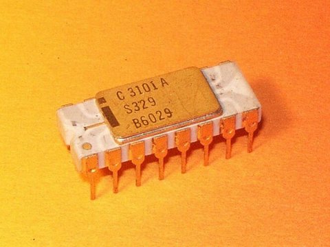
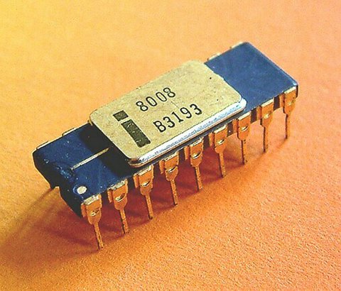
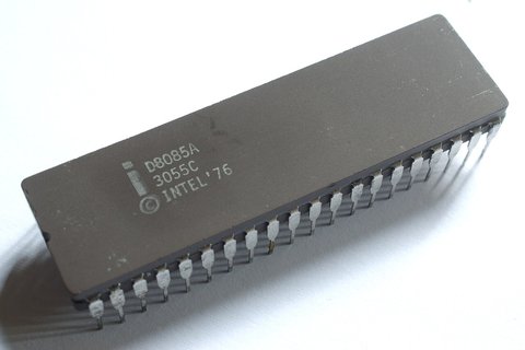
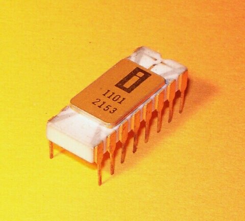
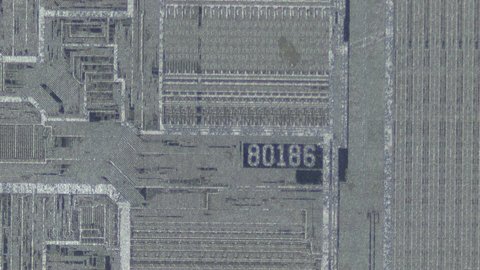
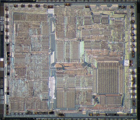
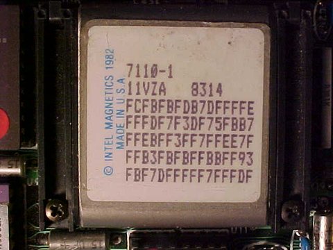
The ceramic Intel 1101 pictured here is the product through which the young company proved that a promising memory technology could survive contact with mass production.
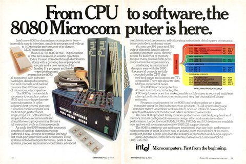
Released in 1969, the 1101 was a 256-bit PMOS static random-access memory. A contemporary advertisement offered it as a 256-by-1 device in a 16-pin package, available from Intel's first facility at 365 East Middlefield Road in Mountain View.
Its importance was larger than its capacity.
The Semiconductor History Museum of Japan identifies the 1101 as the first commercially successful MOS RAM, while Intel describes it as the first high-volume MOS memory made with silicon gates. The qualification matters: Fairchild had already commercialized a silicon-gate integrated circuit, so the honest milestone is Intel's memory process and manufacturability, not a claim to every silicon-gate first.
Manufacturability almost defeated the chip.
Intel's target was about 20 usable die per wafer, but early lots produced roughly two. Process engineer Tom Rowe later called that yield a commercial disaster; design changes kept exposing new defects, and nobody yet knew whether Intel's chosen MOS silicon-gate process could be made dependable.
The breakthrough came from chemistry rather than a new marketing claim.
Gordon Moore and the process team experimented with cleaning and bonding treatments until one chemical dip produced 25 usable die from a wafer. The result turned the 1101 from an elegant laboratory idea into a repeatable manufacturing foundation, and the process knowledge carried forward into the far more successful 1103 DRAM.
The good was foundational: Intel learned how to unite device design, process engineering, and rapid feedback in one small organization. The bad was equally instructive: the 1101 itself began as an uneconomic product, and later memory chips—not this one—created the volume business the founders imagined.
The site also carries a longer industrial cost.
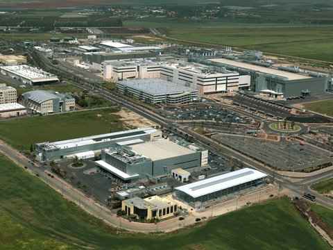
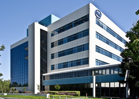
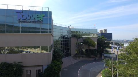
The pin marks Intel's first office and manufacturing facility, where the company operated from 1968 until 1981. The address is now part of the Middlefield-Ellis-Whisman Superfund study area because of historical semiconductor solvents; it is not a visitor attraction, and the exterior should be viewed only from public streets.
Photo: Christian Bassow, CC BY-SA 4.0, via Wikimedia Commons.















changes?
delete this memory?
We detected that you have a Blox in your crypto wallet! We will import the Blox into your account.
Click on done below to complete the import.
Welcome Back!
Sign in to preserve cherished moments
Don't have an account?
Welcome!!
Sign up and start preserving cherished moments
?
?




Choose your payment method
Buy with Metablox Credit
Do you want to mint Blox with Metablox Credit?
Which Crypto would you like to use?
Purchase Confirmed!
Your Blox is being minted on-chain and will appear in your profile shortly.
Log in or sign up to claim your Blox.
How many credits do you want to buy?
$100 USD = 1 Metablox Credit = 1 Blox.
Use Metablox Credit to mint any Blox you want on the map.
 expand_more